How to Recognize a Good Solder Joint
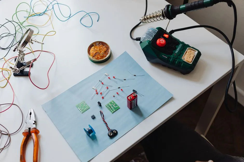
A good joint satisfies electrical and mechanical needs
Appearance helps, but a reliable solder joint also needs correct wetting, sufficient intermetallic bond, appropriate solder volume, preserved pad and lead, no bridges, proper component position, and acceptable electrical behavior. Alloy, flux, surface finish, lead-free process, and joint geometry affect color and texture.
Do not use “shiny” as a universal pass rule. Some good lead-free joints look more matte than familiar tin-lead work.
Look for smooth wetting boundaries
Solder should transition onto both pad and lead rather than sitting as a rounded bead on one surface. The joint outline should allow inspection of the lead and land instead of hiding them under a sphere. Through-hole solder should fill and wet according to the assembly requirement; surface-mount joints should retain alignment and specified fillet.
Use magnification and angled light after the board cools.
Recognize common defect clues
Poor wetting can produce a blob with a visible boundary. Too little solder may leave incomplete coverage or weak attachment. Too much hides the interface and can bridge adjacent pads. Movement during cooling can create a disturbed surface. Excess dwell can darken laminate, lift pads, melt connectors, or damage components.
Cracks, rings around leads, spikes, solder balls, exposed whiskers, shifted parts, tombstoned chips, and burnt residue deserve investigation.
Do not reflow blindly
Before reheating, identify whether the cause was contamination, oxidized tip, insufficient flux, wrong alloy, poor thermal contact, component movement, damaged pad, or a heat-sinking plane. Adding solder repeatedly can increase bridges and thermal damage while leaving the original interface untouched.
Use tip preparation and compatible flux. Stop when the board or component exceeds its process limits.
Inspect adjacent structures
Check neighboring pins, vias, solder mask, traces, plastic housings, wire insulation, and underside. A joint can look acceptable from one direction while a bridge hides behind the lead. Confirm polarity and orientation before celebrating the fillet.
Clean only through the flux-specific process so residue does not conceal fine bridges or corrosion.
Test with power removed
After handling stored energy safely, use continuity and resistance checks to confirm the intended net and absence of adjacent shorts. In-circuit paths can complicate readings; compare with the schematic rather than expecting every neighboring pin to be open.
Mechanical testing should be appropriate to the assembly. Do not pry a joint or wiggle fragile pads to prove strength.
Verify under controlled power
Power the known isolated low-voltage circuit through an appropriate current limit. Monitor total current, rail voltage, signal behavior, and temperature. A joint that passes continuity may still have enough resistance to fail under load or movement.
Use a documented voltage-drop or waveform test when the circuit requires it, with probes secured before power where possible.
Know when the pad is already damaged
If a land lifts, via pulls out, laminate chars, or trace separates, stop heating. A repair may require a qualified board-rework method, anchored conductor, replacement board, and restored clearance or strain relief. A floating pad cannot be convinced back into service by a larger solder sculpture.
Judge the process, not a single photograph
Record tip, alloy, flux, temperature setting, dwell pattern, and cleanup. If several joints share the same defect, correct the process before touching each one. Consistency is the useful beauty standard: good wetting, right amount, intact board, correct circuit, repeatable result.